TSMC, the leader of wafer foundry, recently held an annual technology forum to announce that the 3-nanometer N3 process will enter mass production in the second half of the year as scheduled, and tsmcfinflex technology supporting N3 will be launched, further improving the performance, power consumption efficiency and density of the 3-nanometer family technology.

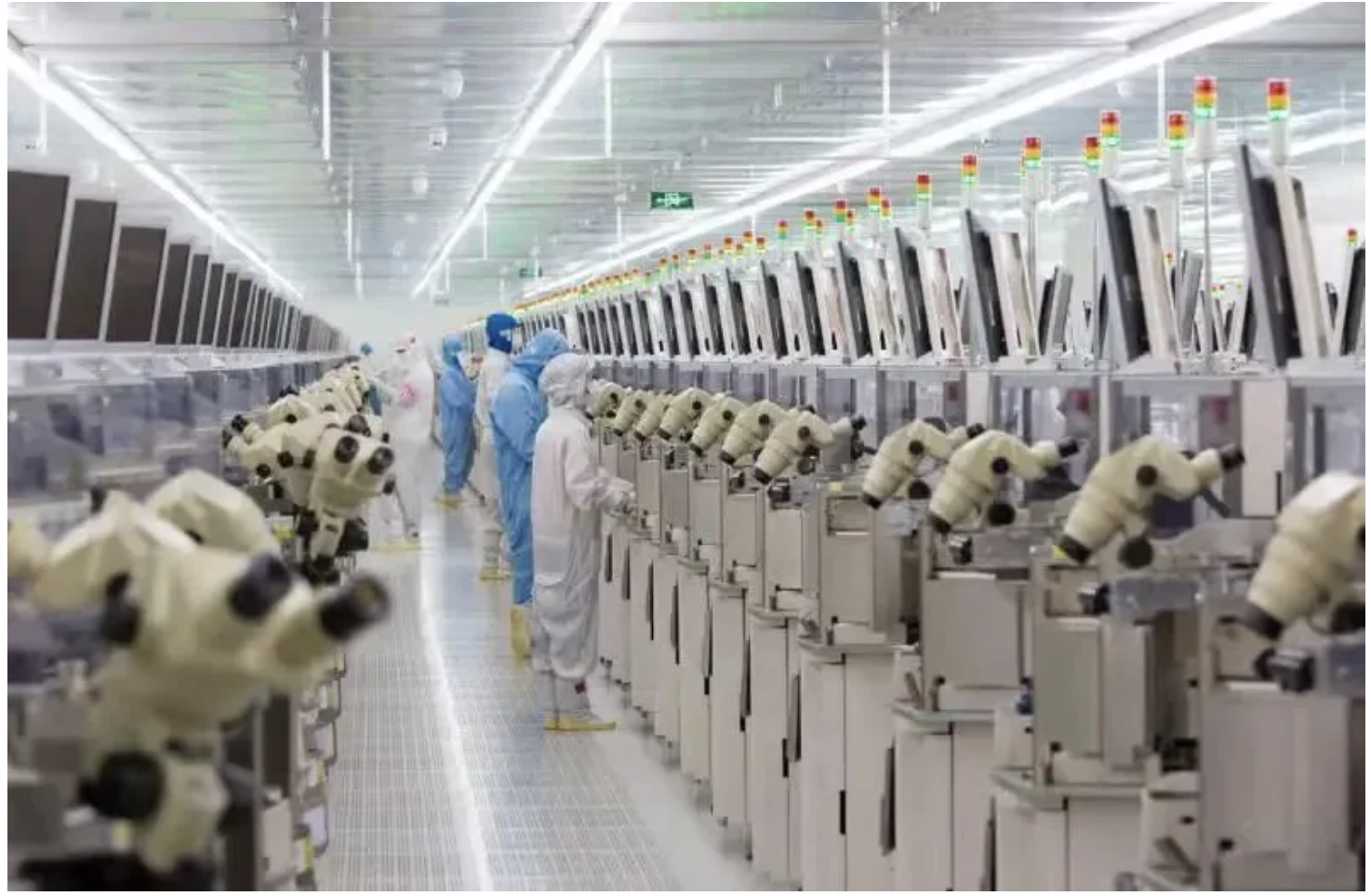
TSMC today (17) announced two major breakthroughs made by 3dfabric platform at the 2022 North American technology forum, and said that TSMC's first fully automated 3dic advanced packaging plant in the world would be mass produced in the second half of the year.

On the surface, M1 ultra is two M1 Max connected together through the chip to chip connector of ultrafusion. The connector itself is very powerful: with a chip to chip bandwidth of 2.5tb/s, the two M1 Max can be logically regarded as a large M1 Ultra.

Recently, Changdian technology said on the interactive platform that the company has been able to realize the packaging of 4nm mobile phone chips, as well as the integrated packaging of CPU, GPU and RF chips, making another breakthrough in advanced packaging technology.
top