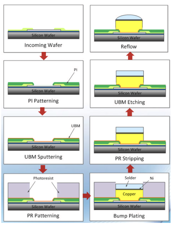
Bumping Process Introduction
Wafer bumping is an essential to flip chip or board level semiconductor packaging. Bumping is an advanced wafer level process technology where “bumps” or “balls” made of solder are formed on the wafers in a whole wafer form before the wafer is being diced into individual chips. Those “bumps”, which can be composed from eutectic, lead free, high lead materials, or Cu pillar on wafer are the fundamental interconnect components that will interconnect the die and the substrate together into a single package. These bumps not only provide a connected path between die and substrate, but also play an important role in the electrical, mechanical and thermal performance in the flip chip package.
Bumping Process Flow

Source: 华进半导体
top