


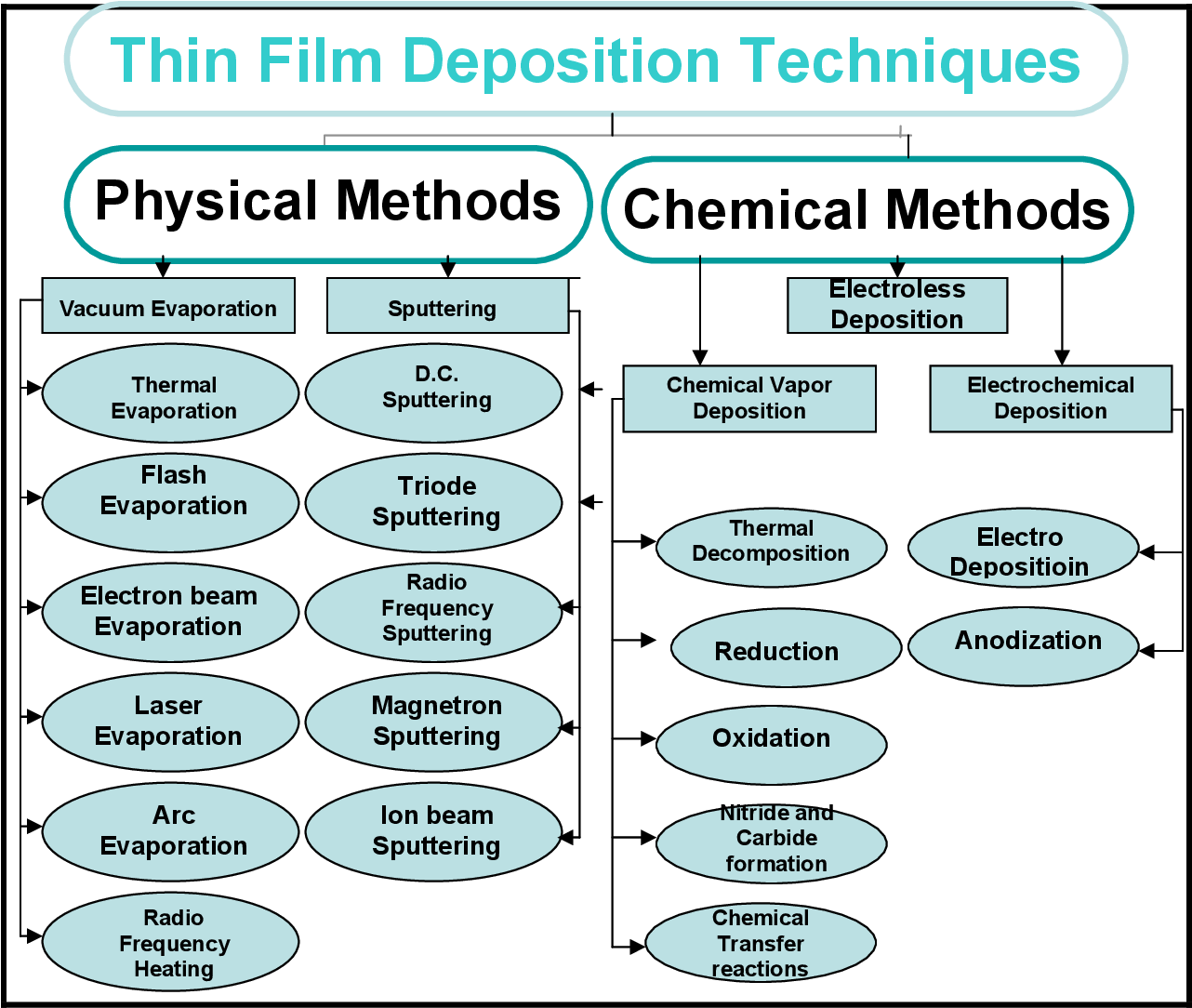
Thin film deposition equipment in semiconductors is mainly divided into two parts, physical vapor deposition equipment (PVD) and chemical vapor deposition equipment (CVD). PVD equipment is mainly used to deposit solid materials on the wafer surface by means of thermal evaporation or magnetron sputtering to convert them into atoms or ions. The equipment needs to have high requirements on the distribution of electric field, magnetic field and thermal field. The CVD equipment reacts with different gases into the equipment cavity to generate thin films with different thicknesses and properties. There are many kinds of CVD reactions, including thermal CVD, plasma CVD, especially CVD with plasma, which has high requirements for plasma generation control.
top